

Micro- and nanofabrication
Micro- and nanofabrication makes structures far smaller than a hair: the transistors in a chip, the gears of a watch, the fibers in a filter. Instead of cutting or squeezing bulk material, these processes grow, draw, deposit or remove matter in steps measured in microns (thousandths of a millimeter) or even single atoms.
The big idea
At this scale, ordinary tools are useless: no drill bit is thin enough and no hand is steady enough. So the work is done by light, ions, electric fields and chemistry, which can be focused or controlled far below what the eye can see. Think of it as writing with a beam instead of carving with a knife: the finer the beam, the finer the writing.
Many of these processes run in cleanrooms: rooms whose air is filtered until it holds thousands of times fewer dust particles than ordinary air, with workers in full-body suits. A single speck of dust is far larger than a transistor, so one particle landing on a wafer can ruin a chip.
The 9 processes in this chapter
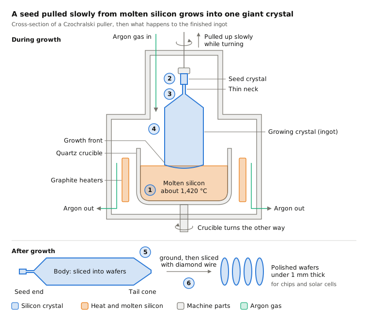
 13.1Czochralski crystal growth (silicon wafers)Pulls a giant single crystal of silicon slowly out of a meltOpen the lesson
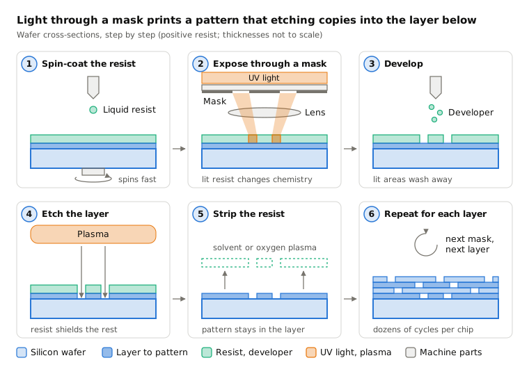
 13.2PhotolithographyProjects a pattern with light onto a light-sensitive coating, then etches itOpen the lesson
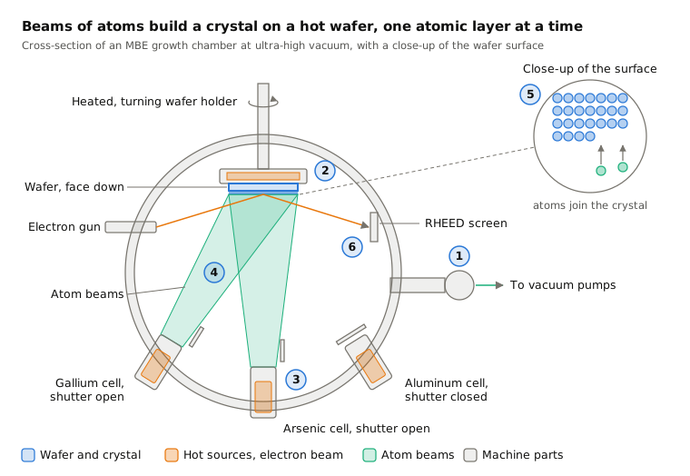
 13.3Molecular beam epitaxy (MBE)Grows a crystal one atomic layer at a time from beams in ultra-high vacuumOpen the lesson
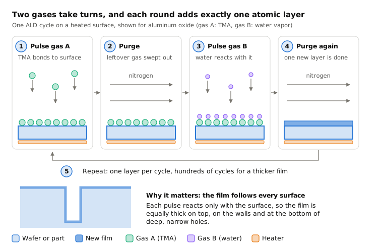
 13.4Atomic layer deposition (ALD)Coats a surface one atomic layer per cycle with alternating gasesOpen the lesson
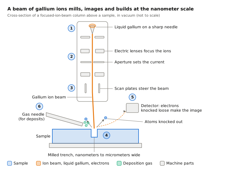
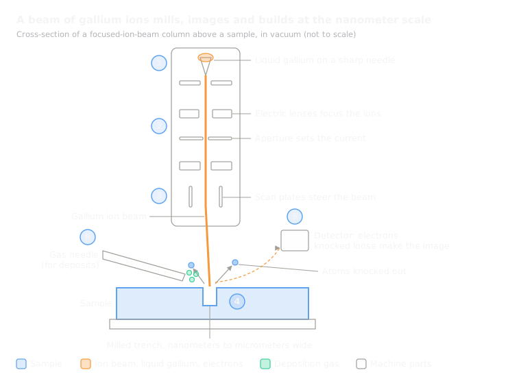 13.5Focused ion beam (FIB)Mills or adds material with a beam of ions under a microscopeOpen the lesson
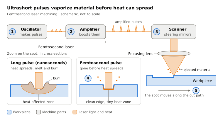
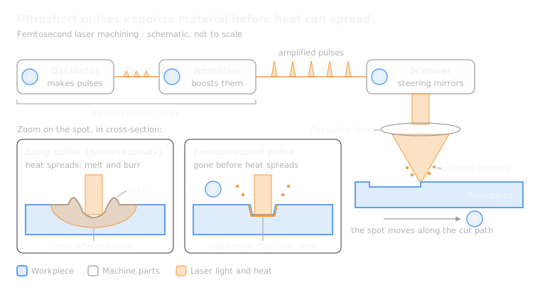 13.6Femtosecond laser machiningRemoves material with ultrashort laser pulses, without meltingOpen the lesson
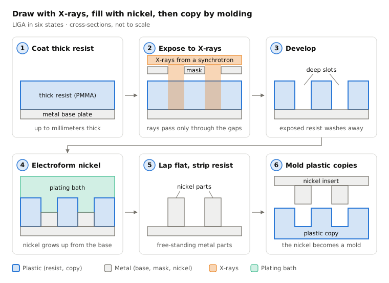
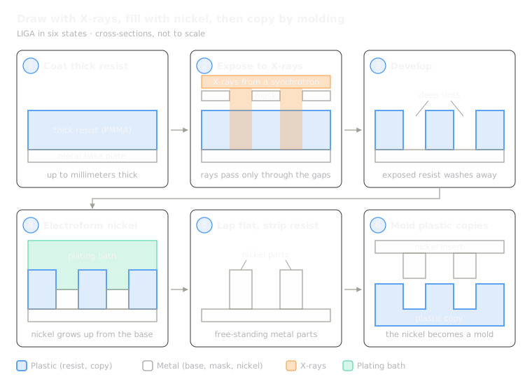 13.7LIGADraws deep slots with X-rays or UV, fills them with nickel, then molds copiesOpen the lesson
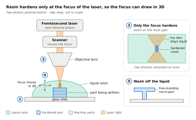
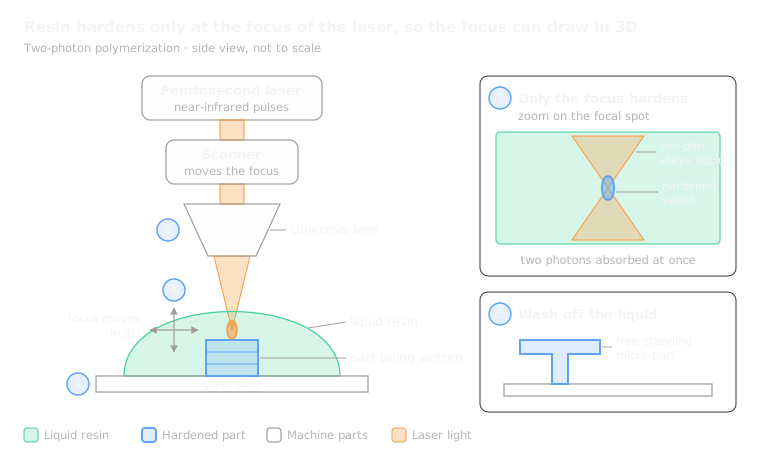 13.8Two-photon polymerizationHardens resin only at a laser focus to print 3D micro-partsOpen the lesson
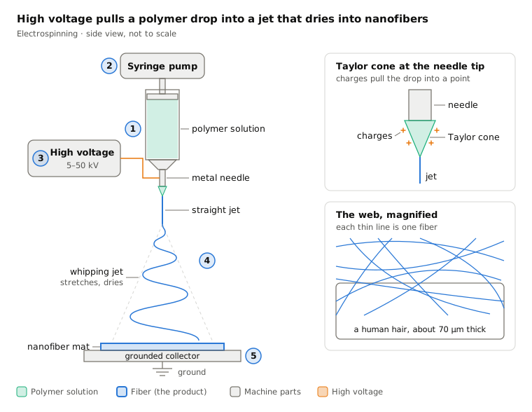
 13.9ElectrospinningPulls a polymer jet into nanofibers with high voltageOpen the lesson
Side by side
| Process | In one line | Best for | Batch size | Precision |
|---|---|---|---|---|
| 13.1Czochralski crystal growth (silicon wafers) | Pulls a giant single crystal of silicon slowly out of a melt | Silicon wafers for chips and solar cells | Continuous production of ingots | A near-perfect crystal, sliced into wafers up to 300 mm across |
| 13.2Photolithography | Projects a pattern with light onto a light-sensitive coating, then etches it | Computer chips, sensors, MEMS | Mass production, millions of chips | Features down to tens of nanometers |
| 13.3Molecular beam epitaxy (MBE) | Grows a crystal one atomic layer at a time from beams in ultra-high vacuum | Lasers, LEDs, fast transistors, research | Small batches of wafers | Single atomic layers |
| 13.4Atomic layer deposition (ALD) | Coats a surface one atomic layer per cycle with alternating gases | Ultra-thin films in chips, coatings inside deep holes | High-volume chip production | About a tenth of a nanometer per cycle |
| 13.5Focused ion beam (FIB) | Mills or adds material with a beam of ions under a microscope | Repairing chips, preparing samples, prototypes | One-offs | Down to about 10 nanometers |
| 13.6Femtosecond laser machining | Removes material with ultrashort laser pulses, without melting | Stents, glass cutting, micro-holes | Prototypes to large series | A few microns |
| 13.7LIGA | Draws deep slots with X-rays or UV, fills them with nickel, then molds copies | Watch parts, micro-gears, micro-molds | Small to medium; plastic copies in large series | Sub-micron, very tall straight walls |
| 13.8Two-photon polymerization | Hardens resin only at a laser focus to print 3D micro-parts | Micro-optics, cell scaffolds, prototypes | One-offs and small series | Sub-micron detail |
| 13.9Electrospinning | Pulls a polymer jet into nanofibers with high voltage | Filters, wound dressings, tissue scaffolds | Lab samples to roll-to-roll lines | Fibers tens of nanometers to a few microns thick |
How to choose within this family
- Making the base material for chips? Silicon crystals come from Czochralski growth, and the finest crystal layers from MBE.
- Patterning millions of identical flat devices: photolithography; adding films a few atoms thick: ALD.
- Fixing, cutting or inspecting one tiny spot: focused ion beam; machining micro-features in metal or glass: femtosecond laser.
- Tall metal micro-parts with straight walls: LIGA; true 3D micro-shapes: two-photon polymerization.
- Large areas of fine fiber web, cheaply: electrospinning.
Key words
- Micron (µm)
- a thousandth of a millimeter; a hair is about 70 µm wide.
- Nanometer (nm)
- a thousandth of a micron; a few atoms side by side.
- Wafer
- a thin, polished disc of crystal, usually silicon, on which chips are built.
- Resist
- a coating that light, X-rays or electrons change chemically, used as a stencil.
- Cleanroom
- a room with heavily filtered air, kept almost free of dust.
- Vacuum chamber
- a sealed box pumped empty of air, so atoms and beams travel freely.
- MEMS
- micro-electro-mechanical systems, tiny machines and sensors built on chips.
- Voxel
- a 3D pixel, the smallest volume a process can form at once.
Try it
Put AI to work in your CAD.
Model parts, generate drawings and automate the repetitive work inside your CAD software.