

Molecular beam epitaxy (MBE)
Grows a crystal one atomic layer at a time from beams in ultra-high vacuum
Molecular beam epitaxy (MBE) grows a crystal one layer of atoms at a time. In a vacuum emptier than the space where the International Space Station flies, small ovens fire beams of pure elements at a hot wafer, and the atoms settle into its crystal grid. It builds the ultra-thin layers inside many lasers and high-frequency chips.
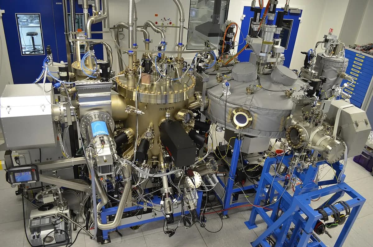
How it works
Pump down. The wafer enters through a load lock (a small airlock), so the main chamber never opens to air. Pumps and cryopanels (surfaces chilled with liquid nitrogen that trap stray gas) hold an ultra-high vacuum, around 10⁻¹⁰ Torr: roughly a ten-trillionth of normal air pressure.
Heat and clean the wafer. The wafer sits face down on a heated, slowly turning holder. Heating drives off its thin oxide skin and leaves an atomically clean crystal surface.
Heat the cells. Effusion cells (small ovens, also called Knudsen cells) hold ultra-pure elements such as gallium, aluminum and arsenic. Heated precisely, each one gives off a steady stream of atoms.
Open the shutters. In such a vacuum, atoms fly in straight lines without hitting anything, like spray paint in empty space. Each cell has a shutter that opens or closes in a fraction of a second, switching materials on and off.
Build the crystal layer by layer. Atoms landing on the hot wafer move around briefly, then lock into place, copying the crystal grid below; this copying is what epitaxy means. Growth runs at about one atomic layer per second, roughly a micrometer per hour.
Count the layers live. RHEED (reflection high-energy electron diffraction) sends an electron beam grazing across the surface onto a glowing screen. The pattern's brightness pulses once per completed atomic layer, so operators can count layers as they grow.
Key facts
- Materials
- Compound semiconductors such as gallium arsenide (GaAs), aluminum gallium arsenide and indium phosphide; also silicon-germanium, oxides and new 2D materials
- Typical parts
- Wafers carrying stacks of crystal layers, some only a few atoms thick, for lasers and transistors
- Part size
- Wafers typically 50–150 mm across; layers from one atom (about 0.3 nm) to a few micrometers thick
- Precision
- Thickness controlled to a single atomic layer, with very sharp boundaries between materials
- Surface finish
- Mirror-smooth, atomically flat
- Batch size it suits
- Research and high-value production; production machines grow a handful of wafers per run
- Tooling and machine cost
- No part-specific tooling; a system typically costs from several hundred thousand to a few million dollars
- Speed
- About one atomic layer per second (roughly 1 µm per hour); a full device stack takes hours
Strengths and limits
Strengths
- Atomic-layer control of thickness and composition
- Extremely pure material with sharp interfaces
- Live monitoring with RHEED
- Makes quantum wells, quantum dots and brand-new materials
Limits
- Very slow growth
- Ultra-high vacuum means long pump-downs, bake-outs and upkeep
- Expensive machines and ultra-pure source materials
- Lower output than MOCVD (metal-organic chemical vapor deposition), the gas-based method used for volume
Where it's used
- PhotonicsLaser diodes, VCSELs (tiny lasers for face recognition and data links), quantum-cascade lasers
- Telecom and radioHigh-frequency transistors (HEMTs) for 5G, satellites and radar
- OptoelectronicsInfrared detectors, photodiodes
- Quantum technologiesQuantum dots, materials for qubits
- ResearchNew materials, 2D crystals, oxide layers
How to recognize it
- You can't see it. MBE layers are a few atoms to a few micrometers thick, buried inside chips smaller than a grain of rice. Only an electron microscope reveals the stacked rows of atoms.
- Where it hides. The lasers in phone face-recognition sensors, fiber-optic transmitters and satellite radio amplifiers rely on epitaxial layer stacks, grown either by MBE or by its gas-based cousin, MOCVD. Nothing on the outside tells you which.
- A finished wafer looks like a plain mirror; nothing shows the dozens of layers inside.
- In lab photos, look for a shiny steel chamber bristling with ports, ovens pointing up at its center and a glowing RHEED screen.
Compare with
Watch it
Dr. Rahat Batool · The principle: ultra-high vacuum, effusion cells, shutters and the heated wafer
AVS - Science and Technology of Materials, Interfaces, and Processing · An expert talk on what growing materials atom by atom makes possible
UoM_EEE · A tour of real MBE machines in a university lab
Anthony Aiello · A live RHEED pattern recorded during growth
See real photos
- Wikipedia: Molecular-beam epitaxy — principle, equipment and history; few photos, so use Commons below
- Wikimedia Commons photo search
Remember
- MBE fires beams of pure atoms at a hot wafer in ultra-high vacuum.
- The new layers copy the wafer's crystal grid, one atomic layer at a time.
- It is slow and costly, but it controls layers down to a single atom.
More in Micro- and nanofabrication
All 100 processes
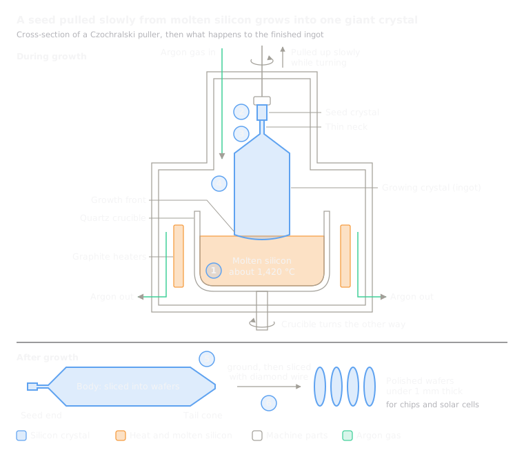 13.1Czochralski crystal growth (silicon wafers)Pulls a giant single crystal of silicon slowly out of a meltOpen the lesson
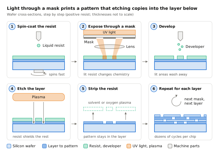
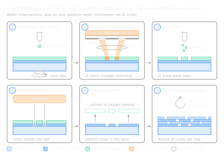 13.2PhotolithographyProjects a pattern with light onto a light-sensitive coating, then etches itOpen the lesson
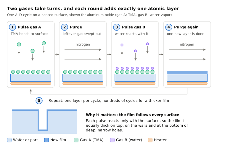
 13.4Atomic layer deposition (ALD)Coats a surface one atomic layer per cycle with alternating gasesOpen the lesson
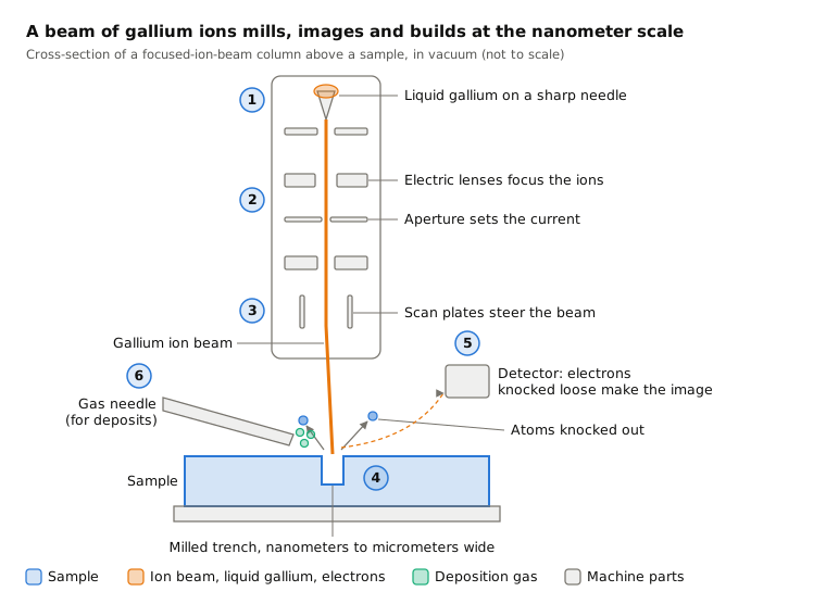
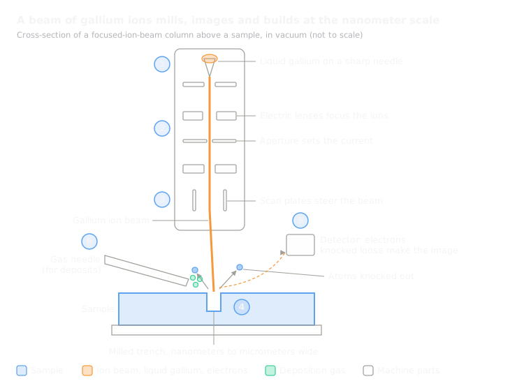 13.5Focused ion beam (FIB)Mills or adds material with a beam of ions under a microscopeOpen the lesson
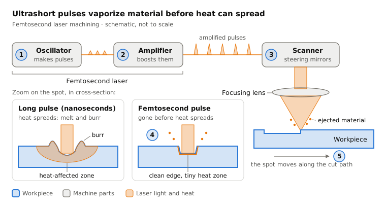
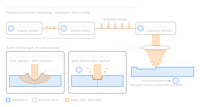 13.6Femtosecond laser machiningRemoves material with ultrashort laser pulses, without meltingOpen the lesson
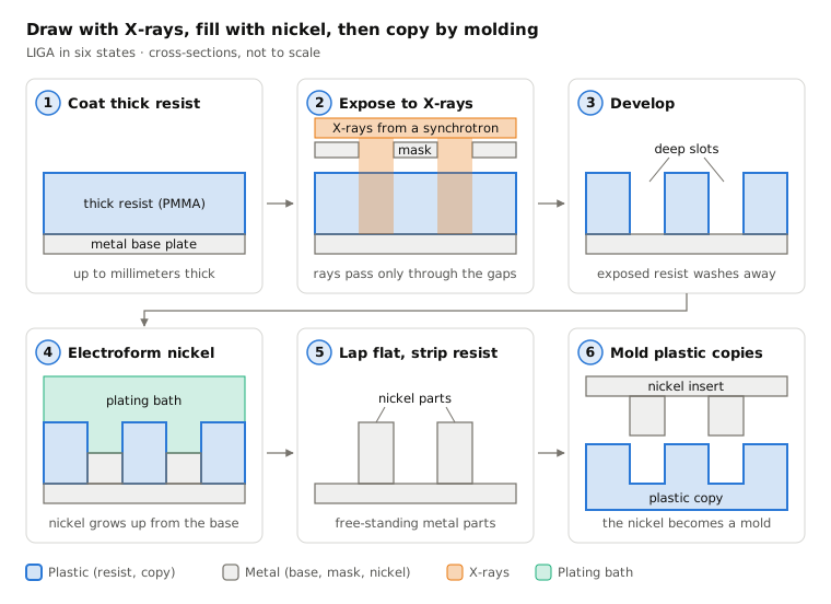
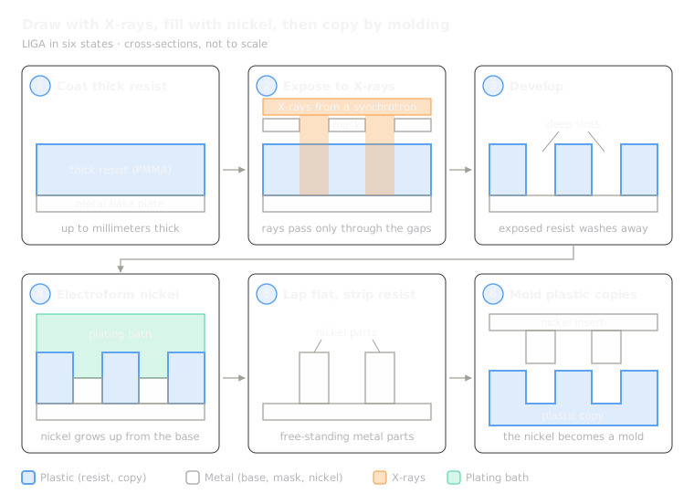 13.7LIGADraws deep slots with X-rays or UV, fills them with nickel, then molds copiesOpen the lesson
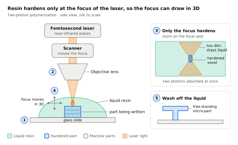
 13.8Two-photon polymerizationHardens resin only at a laser focus to print 3D micro-partsOpen the lesson
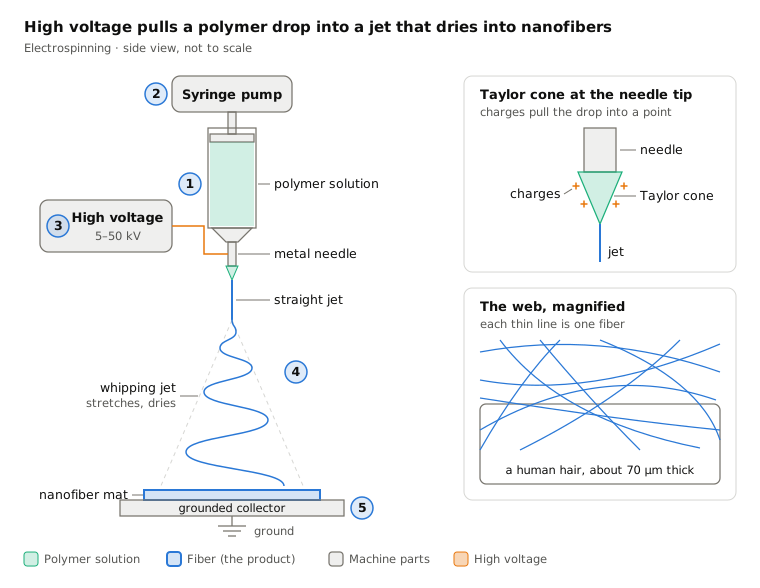
 13.9ElectrospinningPulls a polymer jet into nanofibers with high voltageOpen the lesson
Try it
Put AI to work in your CAD.
Model parts, generate drawings and automate the repetitive work inside your CAD software.