

Focused ion beam (FIB)
Mills or adds material with a beam of ions under a microscope
A focused ion beam (FIB) is a nano-scale sandblaster: a beam of gallium ions, focused to a spot a few nanometers wide, knocks atoms off a surface one tiny area at a time. The same beam can also take pictures and, with a little gas, build tiny metal structures. Chip makers use it to cut open and repair chips, and scientists use it to slice samples thin enough for electron microscopes.
How it works
Make ions. Liquid gallium wets a needle with a very sharp tip. A strong electric field pulls gallium ions (atoms that have lost an electron, so they carry an electric charge) off the tip.
Accelerate and focus. The ions are accelerated, typically to about 30 kV, and electric lenses (charged rings that bend the paths of charged particles) squeeze them into a spot as small as a few nanometers. An aperture (a small hole) sets how many ions get through: more ions cut faster but make a wider spot.
Scan. Scan plates steer the beam across the surface in a programmed pattern, like a tiny CNC tool path.
Mill. Each ion hits the surface like a microscopic cannonball and knocks out a few atoms. This is called sputtering. Pass after pass, the beam digs trenches, holes or cross-sections with walls accurate to tens of nanometers.
Image. The impacts also knock electrons loose. A detector collects them to build a picture, like a scanning electron microscope; most machines also carry a true electron column for gentler imaging.
Deposit or lift out. A needle sprays a gas containing platinum or tungsten. Where the beam hits, the gas breaks down and leaves a metal deposit, used to rewire chips or to weld a thin slice to a tiny probe and lift it out.
Key facts
- Materials
- Almost anything in a vacuum: silicon, metals, ceramics, glass, polymers, frozen biological samples
- Typical parts
- Chip cross-sections and repairs, thin slices (lamellae) for electron microscopes, nano-patterns, tiny probe tips
- Part size
- Features from about 10 nm to tens of micrometers, on samples of a few millimeters to a whole wafer
- Precision
- About ten to a few tens of nanometers
- Surface finish
- Very smooth cut faces; the surface keeps some implanted gallium and a thin damaged layer
- Batch size it suits
- One-offs: analysis, repairs, prototypes
- Tooling and machine cost
- No tooling; instruments cost from several hundred thousand to a few million dollars
- Speed
- Very slow: removing a cube a few micrometers across can take minutes to hours
Strengths and limits
Strengths
- Cuts exactly where you choose, at the nanometer scale, with no mask
- Mills, images and deposits in the same machine
- Works on almost any solid material
- Can repair or rewire a finished chip
Limits
- Extremely slow; only tiny volumes
- Gallium ions implant into and damage the surface
- Expensive instrument, vacuum and skilled operator
- Serial, one point at a time: unsuited to production
Where it's used
- SemiconductorsFailure analysis, cross-sections of faulty chips, circuit edits on prototypes
- MicroscopyThin slices for transmission electron microscopes
- Materials science3D "slice and view" imaging of metals, batteries, rocks
- NanofabricationNano-patterns, nano-pores, tips for probe microscopes
- Life sciencesThin slices of frozen cells (cryo-FIB)
How to recognize it
- You can't see it. FIB cuts are far too small for the eye; you will never spot one on a product. Its work sits behind the chips in your phone and laptop, whose prototypes were cut open, inspected and sometimes repaired with it.
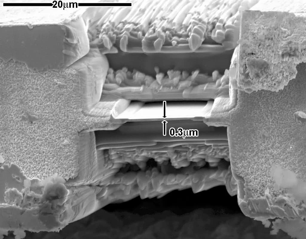
- Under an electron microscope, FIB work shows as perfectly rectangular boxes and trenches with smooth, steep walls, often with a staircase-shaped pit in front of a polished cross-section face.
- Platinum strips. A thin protective metal strip laid on top of a cut area is a typical FIB signature.
Compare with
Watch it
Penn State MRI · A clear lab introduction to the instrument and what it does
AIF NC State University · Milling live, as seen on the operator's screen
Covalent · How a thin slice is cut, welded to a probe and lifted out
PicoScientific · Slice-and-view imaging that rebuilds a sample in 3D
See real photos
- Wikipedia: Focused ion beam — illustrations of the ion column and FIB-made structures
- Wikimedia Commons photo search
Remember
- A focused beam of gallium ions removes atoms exactly where it is aimed.
- The same machine mills, images and deposits metal, all at the nanometer scale.
- It is a tool for analysis, repair and prototypes, far too slow for mass production.
More in Micro- and nanofabrication
All 100 processes
 13.1Czochralski crystal growth (silicon wafers)Pulls a giant single crystal of silicon slowly out of a meltOpen the lesson
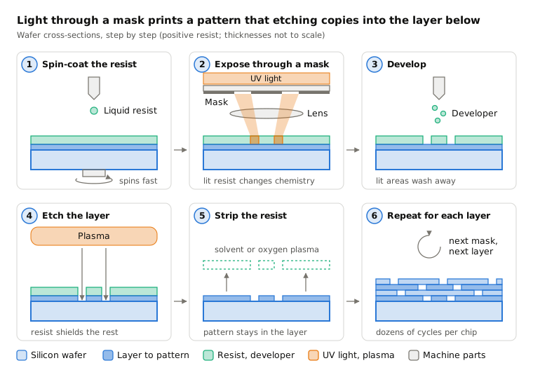
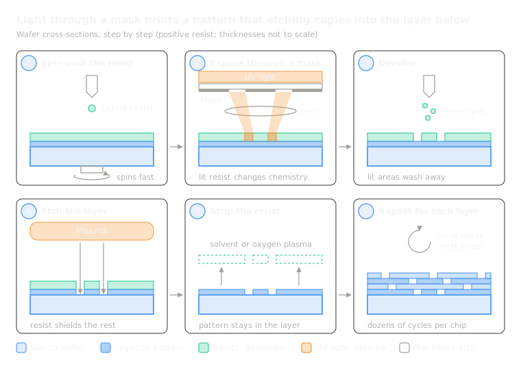 13.2PhotolithographyProjects a pattern with light onto a light-sensitive coating, then etches itOpen the lesson
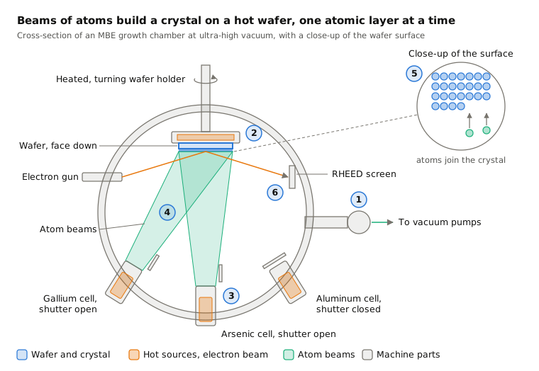
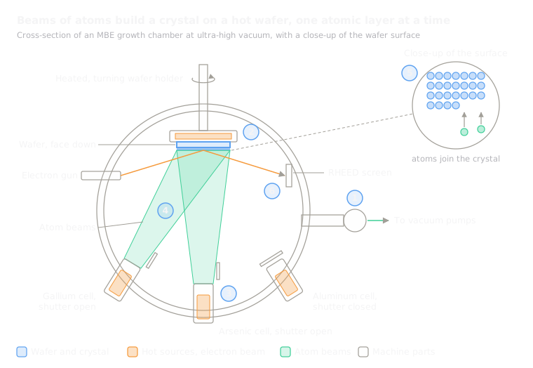 13.3Molecular beam epitaxy (MBE)Grows a crystal one atomic layer at a time from beams in ultra-high vacuumOpen the lesson
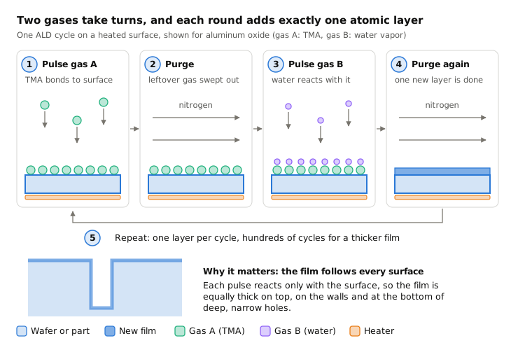
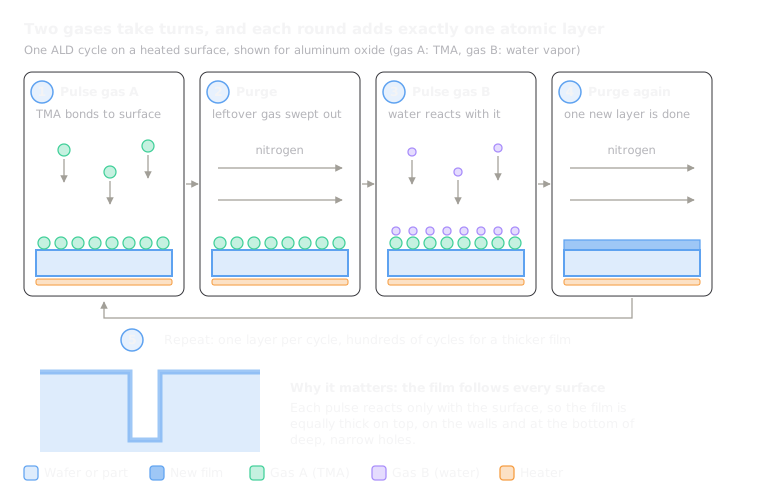 13.4Atomic layer deposition (ALD)Coats a surface one atomic layer per cycle with alternating gasesOpen the lesson
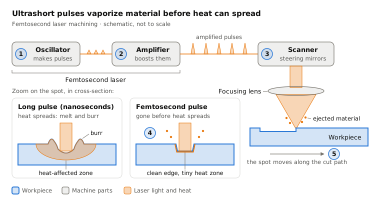
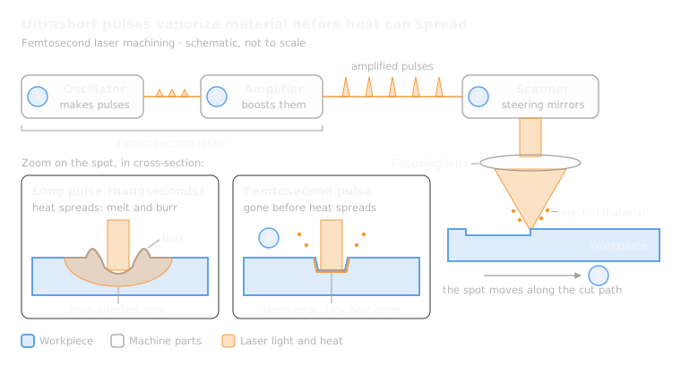 13.6Femtosecond laser machiningRemoves material with ultrashort laser pulses, without meltingOpen the lesson
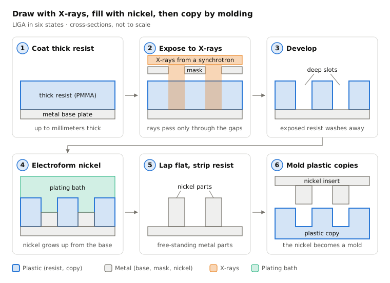
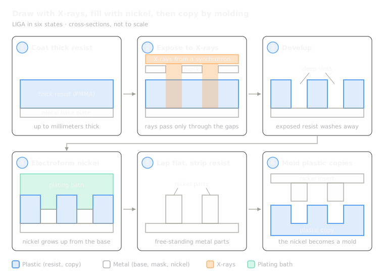 13.7LIGADraws deep slots with X-rays or UV, fills them with nickel, then molds copiesOpen the lesson
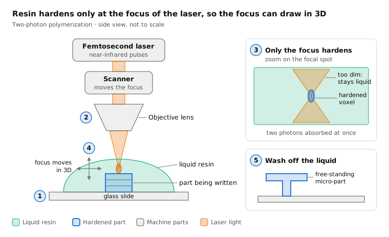
 13.8Two-photon polymerizationHardens resin only at a laser focus to print 3D micro-partsOpen the lesson
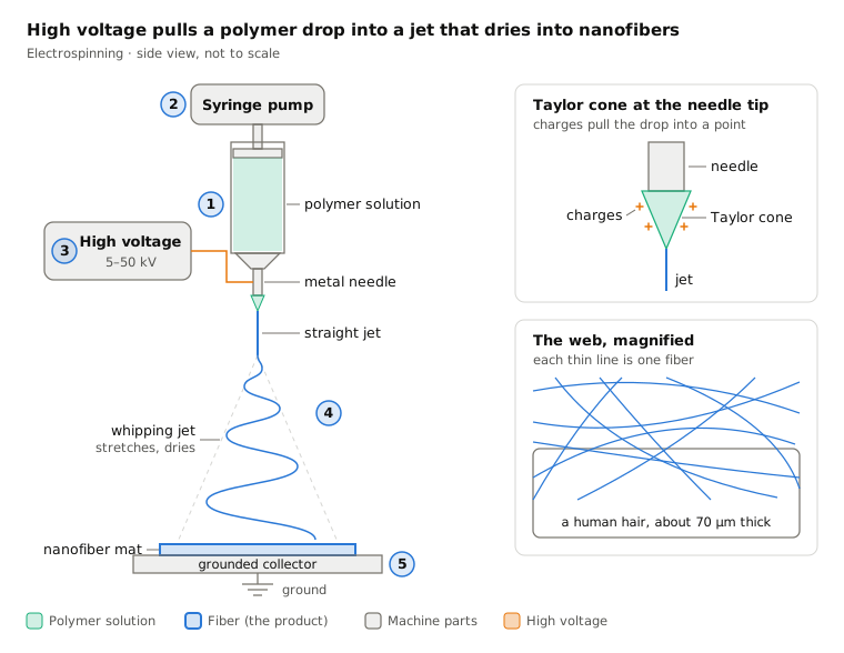
 13.9ElectrospinningPulls a polymer jet into nanofibers with high voltageOpen the lesson
Try it
Put AI to work in your CAD.
Model parts, generate drawings and automate the repetitive work inside your CAD software.