

Atomic layer deposition (ALD)
Coats a surface one atomic layer per cycle with alternating gases
Atomic layer deposition (ALD) grows a film one layer of atoms at a time by letting two gases take turns over a heated surface. Each gas can only react with what the previous one left behind, so every round adds exactly one thin layer, on every surface it can reach. It makes the ultra-thin insulating layers inside modern chips and protective coatings only a few nanometers thick.
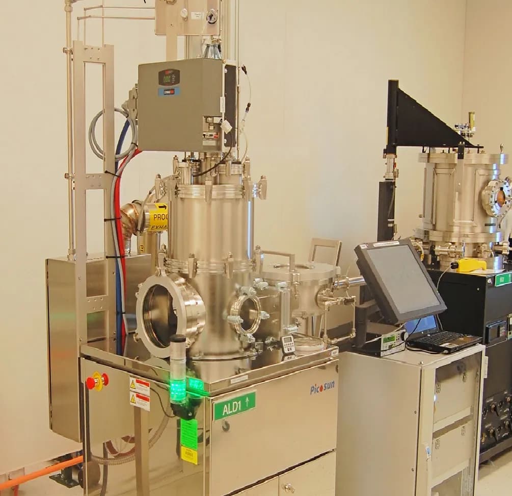
How it works
Pulse gas A. The wafer or part sits in a small chamber, heated to typically 150–350 °C under low pressure. A short puff of the first precursor (a reactive gas that carries the element to deposit), here trimethylaluminum (TMA), bonds to every available spot on the surface. Once every spot is taken, it stops: the reaction is self-limiting.
Purge. Nitrogen or argon sweeps out the leftover gas, so the two precursors never meet in the open space.
Pulse gas B. A puff of the second precursor, here water vapor, reacts with the layer left by gas A and turns it into aluminum oxide. Again it stops by itself when the layer is complete.
Purge again. The byproducts and leftover water are swept out. One cycle is done, and the film is about 0.1 nm thicker: roughly a tenth of a nanometer per cycle.
Repeat. The cycle runs hundreds of times; you choose the thickness simply by counting cycles. A 10 nm film needs roughly 100 cycles, typically taking several minutes to an hour.
Key facts
- Materials deposited
- Oxides (aluminum oxide, hafnium oxide, titanium oxide), nitrides (titanium nitride), some metals; on silicon, glass, metals, polymers and powders
- Typical parts
- Gate insulators and capacitor layers in chips, moisture barriers, coated powders and catalysts
- Part size
- From nanoparticles to 300 mm wafers and batches of wafers or parts
- Precision
- Thickness set to a fraction of a nanometer by counting cycles; even inside holes many times deeper than wide
- Surface finish
- Copies the surface below it exactly, without adding roughness
- Batch size it suits
- Single wafers to large batches; high-volume chip production
- Tooling and machine cost
- No part-specific tooling; lab reactors from roughly $100,000, production tools in the millions
- Speed
- Slow: typically about 0.1 nm per cycle and a few seconds per cycle, so most films stay under about 100 nm
Strengths and limits
Strengths
- Thickness controlled to a fraction of a nanometer
- Perfectly even film, even in deep, narrow holes
- Dense, pinhole-free films at fairly low temperature
- Coats complex 3D shapes and powders
Limits
- Very slow: thick films are impractical
- Precursor gases can be toxic, flammable or costly
- Only some materials have a suitable pair of gases
- Films can trap impurities from the precursors
Where it's used
- MicroelectronicsHafnium-oxide gate insulators in processors, capacitor layers in memory chips
- Displays and flexible electronicsThin barriers that keep moisture out of OLED screens
- EnergyProtective coatings on battery materials, layers in some high-efficiency solar cells
- MEMS and sensorsInsulating and protective coatings on tiny moving parts
- Medical and opticsBiocompatible coatings, anti-reflection layers
How to recognize it
- You can't see it. ALD films are typically a few to a few tens of nanometers thick, thousands of times thinner than a hair. They hide inside the chips of your phone and computer and in the moisture barrier of some OLED screens.
- No color, no texture. A film this thin usually leaves no visible trace; at most, thicker films can shift the color of a surface slightly, like a soap bubble.
- Only a microscope tells. On an electron-microscope cross-section, an ALD film shows as a band of perfectly even thickness that follows every corner and trench.
Compare with
Watch it
HYCOAT ITN · A clear beginner explanation of the ALD cycle
Asianometry · The history of ALD and why chipmakers depend on it
Applied Science · A home-built ALD reactor and a real coated result
Inrfucirvine · A real cleanroom ALD tool being loaded and run
See real photos
- Wikipedia: Atomic layer deposition — schematics of the pulse–purge cycle and of spatial ALD
- Wikimedia Commons photo search
Remember
- Two gases take turns; each turn stops by itself once the surface is covered.
- One cycle adds about a tenth of a nanometer, so thickness is set by counting cycles.
- The film is equally thick everywhere, even deep inside tiny holes.
More in Micro- and nanofabrication
All 100 processes
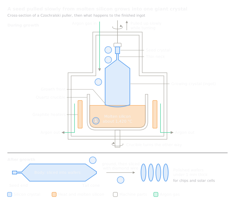 13.1Czochralski crystal growth (silicon wafers)Pulls a giant single crystal of silicon slowly out of a meltOpen the lesson
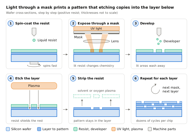
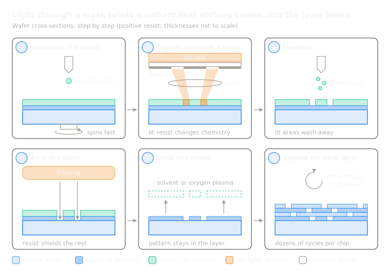 13.2PhotolithographyProjects a pattern with light onto a light-sensitive coating, then etches itOpen the lesson
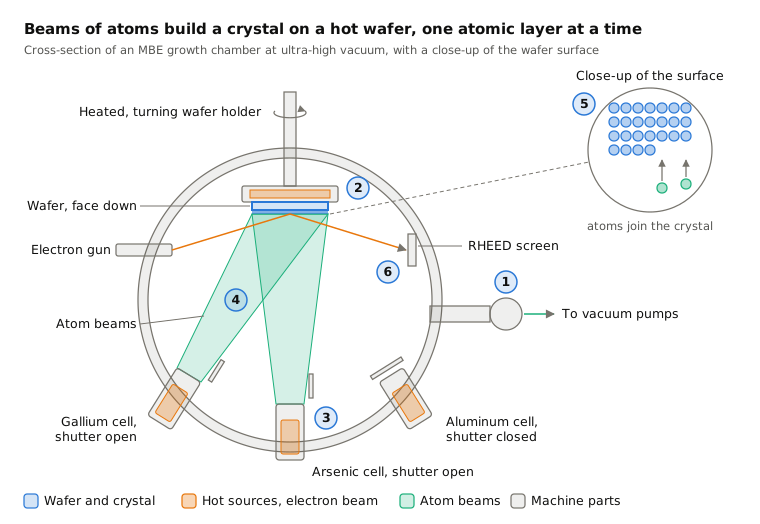
 13.3Molecular beam epitaxy (MBE)Grows a crystal one atomic layer at a time from beams in ultra-high vacuumOpen the lesson
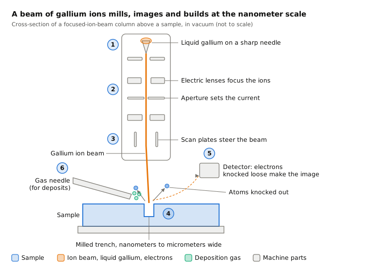
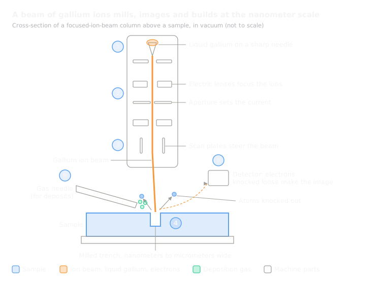 13.5Focused ion beam (FIB)Mills or adds material with a beam of ions under a microscopeOpen the lesson
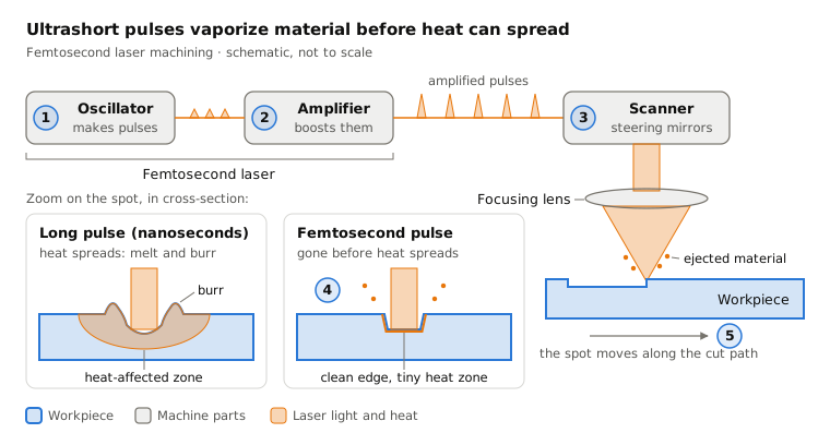
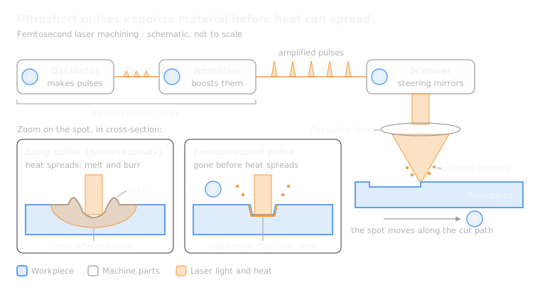 13.6Femtosecond laser machiningRemoves material with ultrashort laser pulses, without meltingOpen the lesson
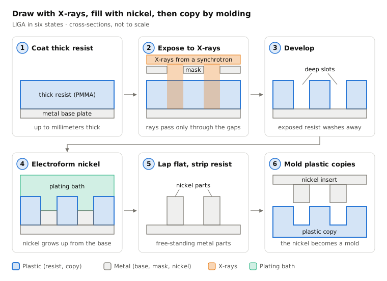
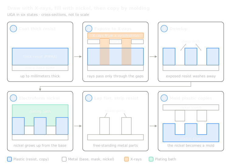 13.7LIGADraws deep slots with X-rays or UV, fills them with nickel, then molds copiesOpen the lesson
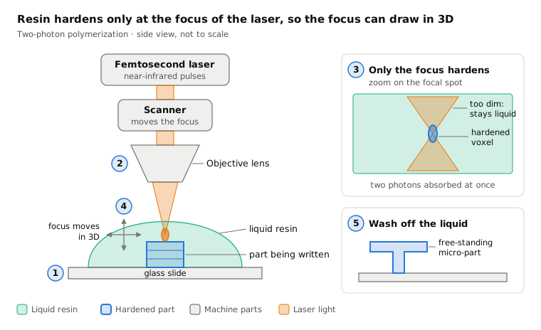
 13.8Two-photon polymerizationHardens resin only at a laser focus to print 3D micro-partsOpen the lesson
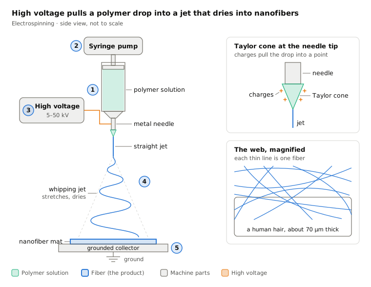
 13.9ElectrospinningPulls a polymer jet into nanofibers with high voltageOpen the lesson
Try it
Put AI to work in your CAD.
Model parts, generate drawings and automate the repetitive work inside your CAD software.