

CVD coating
Gases react on a hot surface and leave a film
CVD (chemical vapor deposition) grows a solid film from gases that react on a hot surface. It lays down the ultra-thin layers inside computer chips and the tough coatings on many carbide cutting inserts. Unlike PVD, the gas reaches into holes and around corners, so every surface gets an even coat.
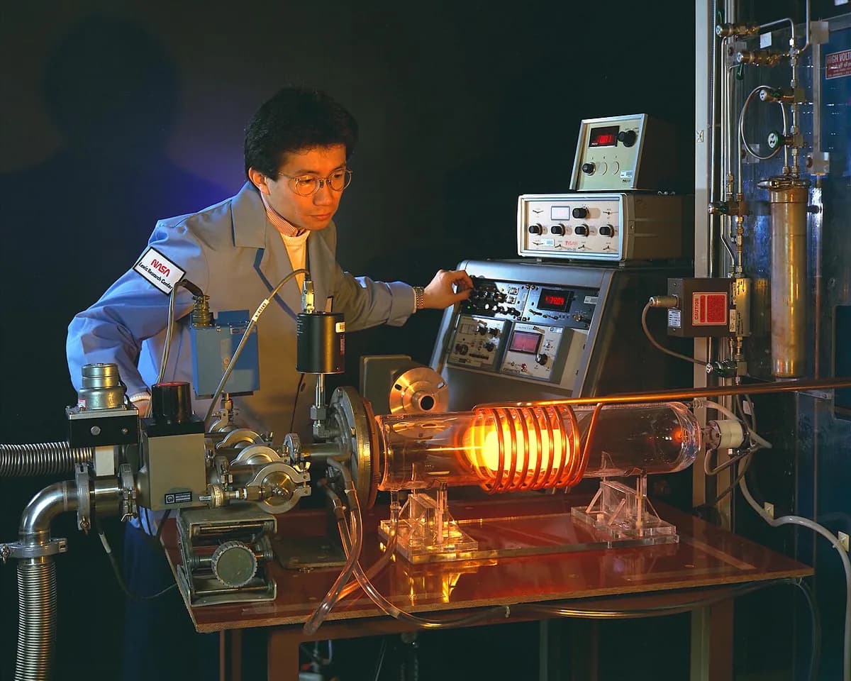
How it works
Load the parts. Wafers (thin silicon discs for chips) or carbide tool inserts are stacked on racks inside the reactor, a sealed tube or chamber.
Heat and feed the gases. The parts are heated, typically to 500–1,100 °C for thermal CVD. Precursor gases flow in: gases that carry the atoms you want, such as silane for silicon or methane for carbon.
React on the hot surface. Near the hot surface the gas molecules break apart and react. The atoms you want stay behind as a solid, tightly bonded film.
Pump away the by-products. Leftover gases, such as hydrogen or acidic hydrogen chloride, are pumped out and cleaned in a scrubber before release.
Grow, then cool. The film thickens evenly on every surface the gas touches, from a few nanometers on chips to about 5–20 µm on tool inserts. The reactor then cools and the parts come out.
Key facts
- Materials
- Films: silicon, silicon oxide and nitride, tungsten, TiN, TiC, alumina, diamond, graphene. Parts: silicon wafers, carbide, ceramics, heat-resistant metals
- Typical parts
- Chip wafers, carbide cutting inserts, solar cells, optical and wear parts
- Part size
- Wafers up to 300 mm across; inserts of a few centimeters; hundreds to thousands of parts per run
- Precision
- Films from a few nanometers to about 20 µm, very uniform, even inside holes and trenches
- Surface finish
- Smooth and dense, copying the surface below; tool coatings look gray, gold or black
- Batch size it suits
- Large batches: hundreds of wafers or thousands of inserts per run
- Tooling and machine cost
- High to very high: industrial reactors cost hundreds of thousands to millions of dollars, chip tools at the top
- Speed
- Slow: a tool-coating run typically lasts many hours; thin chip layers take minutes to hours
Strengths and limits
Strengths
- Coats every surface the gas reaches, even inside holes
- Very uniform, dense films that bond strongly
- Huge range of materials, from silicon to diamond
- Exact nanometer layers for chips, or thick wear layers for tools
Limits
- High heat, often near 1,000 °C, rules out many steels and plastics
- Toxic, flammable or corrosive gases need careful handling
- Expensive reactors and long runs
- Hard to mask: it also coats places you may not want
Where it's used
- ElectronicsInsulating and conducting layers inside chips, solar cells
- Cutting toolsThick TiCN and alumina layers on carbide turning inserts
- OpticsHard and anti-reflective coatings, synthetic diamond windows
- JewelryLab-grown diamonds
- AerospaceAluminide coatings that protect turbine blades from hot gases
- ResearchGraphene sheets and carbon nanotubes
How to recognize it
- An even coating that reaches inside holes, slots and the back side of a part.
- Carbide inserts with a thick gold, gray or black coating whose layers show as bands at a chipped edge.
- The rainbow colors of a silicon wafer: thin films, often CVD-grown, whose thickness sets the color.
- Lab-grown diamond certificates that say CVD.
Compare with
Watch it
Massachusetts Institute of Technology (MIT) · A clear explanation of how CVD works and why it matters
Physics, Materials Science and Nano Lecture Series · The reaction steps on the surface, animated
Physics, Materials Science and Nano Lecture Series · The main variants: at normal pressure, at low pressure, with a plasma
CVDEquipment · What a real plasma CVD machine looks like
See real photos
- Wikipedia: Chemical vapor deposition — reactor types, materials and uses, with links to photos
- Wikimedia Commons photo search
Remember
- CVD grows a solid film from gases that react on a hot surface.
- The gas reaches everywhere, so holes and back sides get an even coat too.
- Chip layers, thick insert coatings and lab-grown diamonds all come from CVD.
More in Coatings and surface finishing
All 100 processes
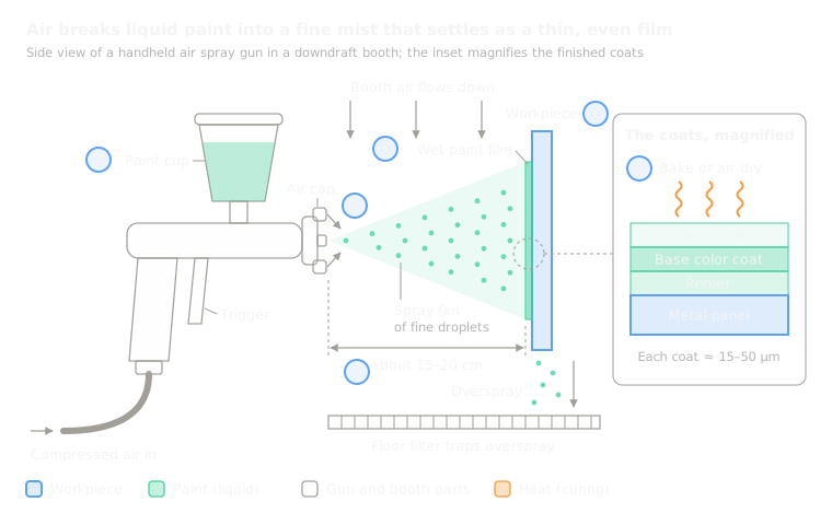 11.1Spray paintingLiquid paint atomized into a fine mist that dries or curesOpen the lesson
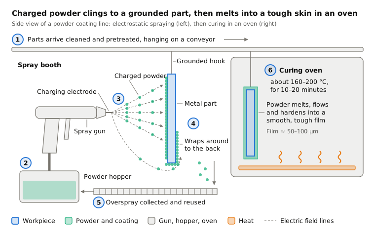
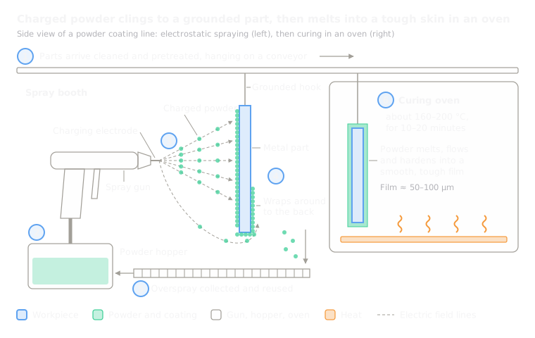 11.2Powder coatingCharged dry powder clings to the part, then melts in an ovenOpen the lesson
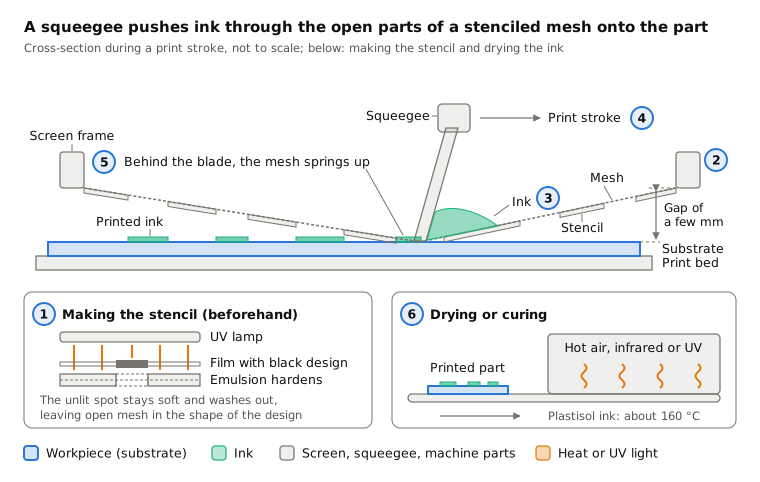
 11.3Screen printingInk pushed through a mesh stencilOpen the lesson
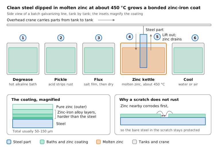
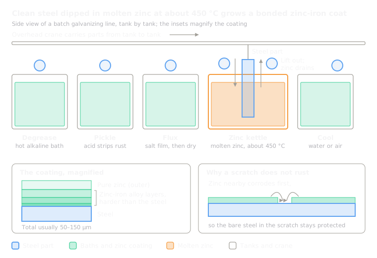 11.4Hot-dip galvanizingSteel dipped in molten zinc forms a bonded zinc layerOpen the lesson
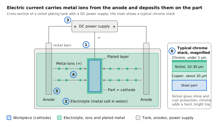
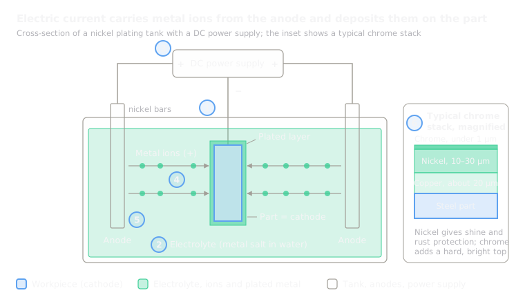 11.5Electroplating (chrome, nickel, zinc)Electric current deposits metal from a bathOpen the lesson
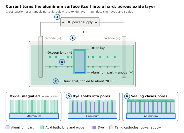
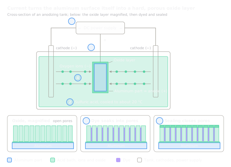 11.6AnodizingCurrent grows a hard oxide out of aluminum itselfOpen the lesson
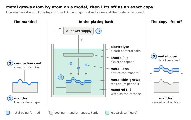
 11.7ElectroformingPlating grown thick on a model, then lifted offOpen the lesson
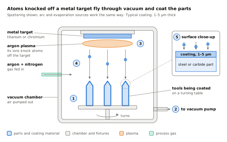
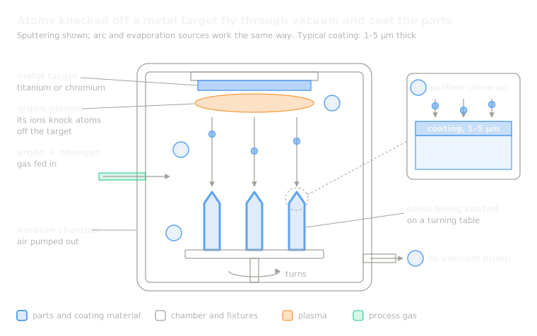 11.8PVD coating (thin films in vacuum)Atoms knocked off a target coat parts in vacuumOpen the lesson
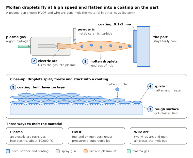
 11.10Thermal spraying (plasma, HVOF, arc)Melted droplets fired at a part stack into a layerOpen the lesson
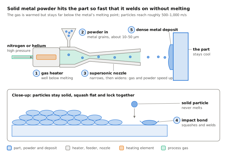
 11.11Cold spraySolid metal grains weld on by sheer speedOpen the lesson
Try it
Put AI to work in your CAD.
Model parts, generate drawings and automate the repetitive work inside your CAD software.