

Czochralski crystal growth (silicon wafers)
Pulls a giant single crystal of silicon slowly out of a melt
Czochralski growth (say "cho-HRAHL-skee") makes a giant single crystal of silicon: one solid piece in which every atom sits in the same perfect grid. A small seed is dipped into molten silicon and pulled up very slowly, and the silicon freezes onto it. Sliced into thin disks called wafers, these crystals are the base of almost every computer chip and of many solar cells.
How it works
Melt the silicon. Chunks of ultra-pure silicon are melted in a quartz crucible (a heat-proof bowl) at about 1,420 °C. A measured pinch of boron or phosphorus (a dopant, which sets how the silicon conducts electricity) goes in too, and argon gas keeps air away from the melt.
Dip the seed. A small seed crystal, cut so its atomic grid points in a chosen direction, is lowered until it just touches the melt. Silicon atoms freeze onto it and copy its grid.
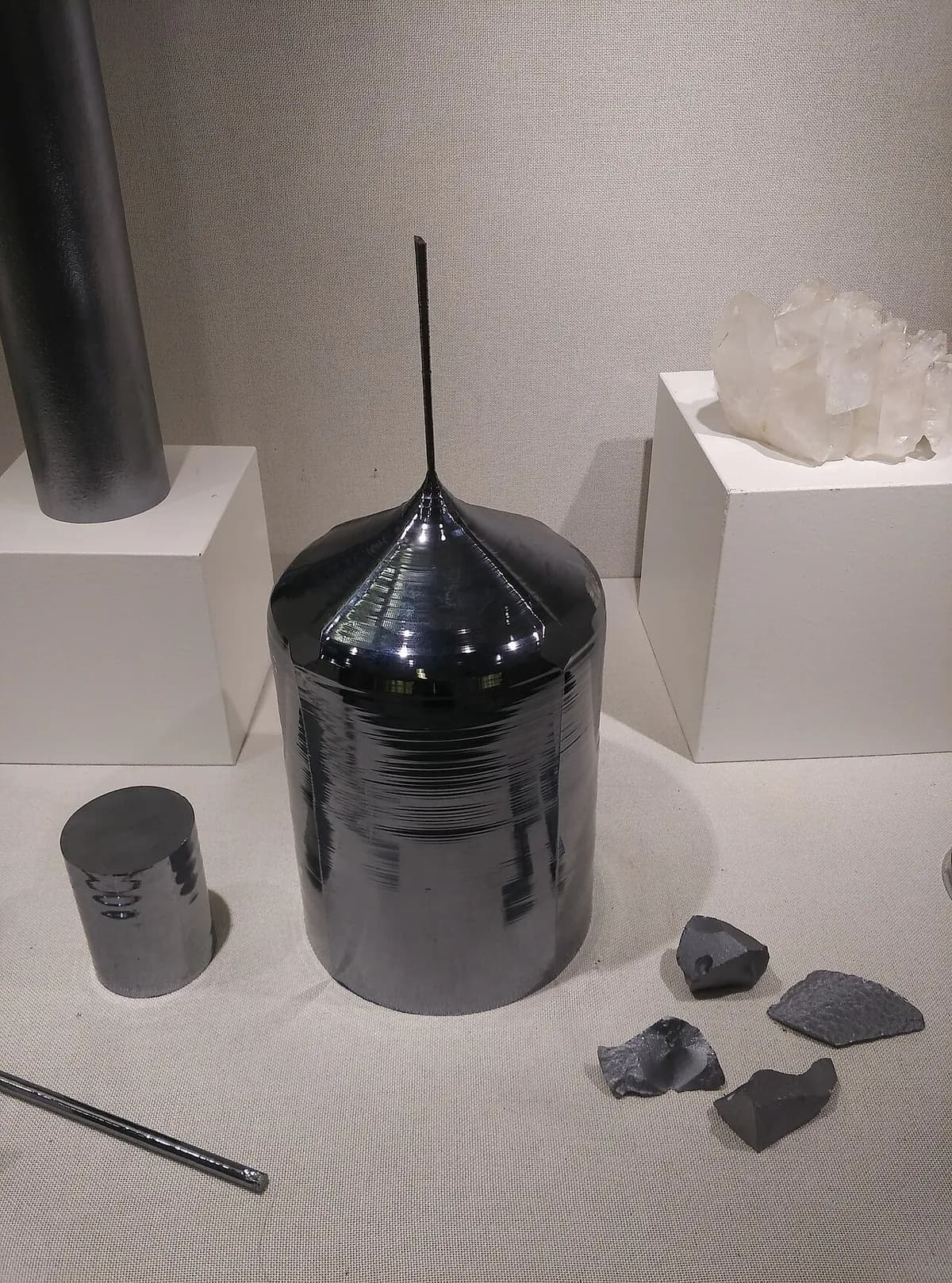
Pull a thin neck. The seed is first pulled up quickly, making a neck only a few millimeters wide. Defects (dislocations, flaws in the atomic grid) grow out through the neck instead of spreading into the crystal.
Grow the shoulder and body. The pull slows, so the crystal widens into a cone (the shoulder), then grows at full diameter, typically 200 or 300 mm. Seed and crucible turn in opposite directions to keep the melt even, and the crystal rises at roughly a millimeter per minute.
Taper the tail and cool. At the end, the diameter is narrowed into a cone so the crystal leaves the melt without a thermal shock (a sudden temperature change that would damage its grid). The finished crystal, called an ingot, is lifted out and cooled slowly.
Grind and slice. The ingot is ground to an exact cylinder and notched to mark its crystal direction. Diamond-coated wire slices it into wafers under 1 mm thick, which are then polished to a mirror finish.
Key facts
- Materials
- Mostly silicon; also germanium and some oxide crystals for lasers and optics
- Typical parts
- Cylindrical ingots (also called boules), sliced into wafers
- Part size
- Typically 200–300 mm in diameter, up to about 2 m long and several hundred kg
- Precision
- One continuous atomic grid without dislocations; diameter held to about a millimeter before grinding; finished wafers flat to about a micrometer (a thousandth of a millimeter)
- Surface finish
- As grown: shiny metallic gray with faint ridges along its length; finished wafers are mirror-polished
- Batch size it suits
- Mass production: each puller grows one ingot at a time, around the clock
- Tooling and machine cost
- A puller costs on the order of a million dollars; the quartz crucible is a consumable, replaced after one or a few ingots
- Speed
- Roughly 1 mm of crystal per minute, so one ingot takes a day or more
Strengths and limits
Strengths
- Huge, nearly perfect single crystals
- Exact doping sets the electrical behavior
- Mature and highly automated, up to 300 mm wafers
- The standard starting point for chips and many solar cells
Limits
- Oxygen from the quartz crucible dissolves into the silicon
- Slow: one ingot can take days
- Uses a lot of energy and consumes crucibles
- The dopant level drifts from one end of the ingot to the other
Where it's used
- ElectronicsProcessors and memory chips, made on 300 mm wafers
- Solar energyMonocrystalline solar cells
- Power electronicsPower transistors and diodes in chargers, cars and trains
- Sensors and MEMS (tiny machines etched in silicon)Phone camera image sensors, motion sensors (accelerometers)
- Optics and lasersGermanium for infrared optics, laser crystals such as Nd:YAG
How to recognize it
- Mostly, you can't. The crystal ends up invisible inside every chip: a small square cut from a wafer, sealed in a black package on the circuit board of your phone or laptop.
- Solar panels. Monocrystalline cells look evenly dark, without a flaky pattern, and often have slightly cut-off corners: they were squared off from a round ingot.
- Bare wafers. A mirror-like gray disk, usually with a small notch or flat on its edge that marks the crystal direction.
- Whole ingots, in factory photos or museums, look like giant gray bullets with faint straight ridges along them that reveal the crystal's internal grid.
Compare with
Watch it
Linton Crystal Technologies · Seeding, necking and pulling, animated inside a puller
Intel · Where the ingot fits on the path from sand to finished chip
Linton Crystal Technologies · Real crystal pullers and finished ingots in a factory
Linton Crystal Technologies · How an ingot is sliced into wafers
See real photos
- Wikipedia: Czochralski method — process illustrations and photos of silicon ingots
- Wikimedia Commons photo search
Remember
- A seed pulled slowly from molten silicon grows into one flawless crystal up to about 2 m long.
- A thin neck, slow pulling, opposite rotations and argon gas keep that crystal perfect and clean.
- Almost every chip and many solar cells start as a slice of such an ingot.
More in Micro- and nanofabrication
All 100 processes
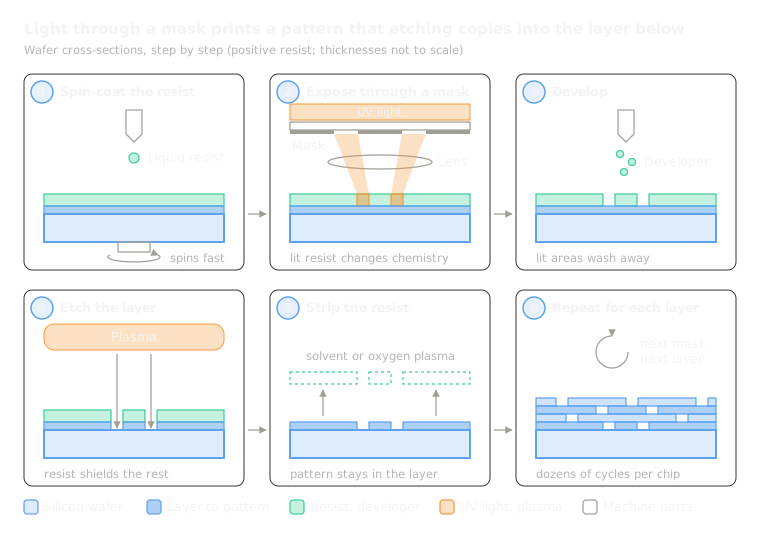 13.2PhotolithographyProjects a pattern with light onto a light-sensitive coating, then etches itOpen the lesson
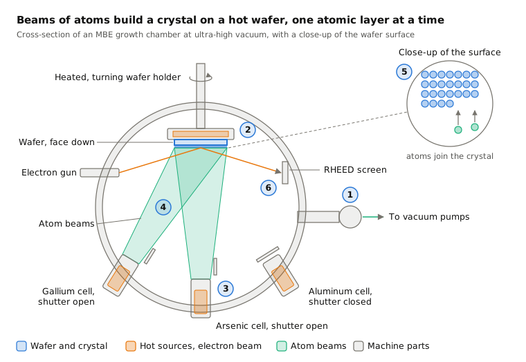
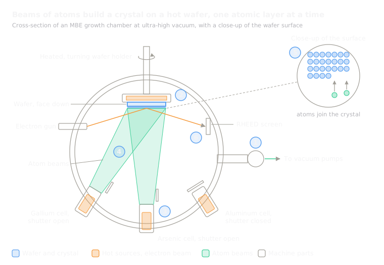 13.3Molecular beam epitaxy (MBE)Grows a crystal one atomic layer at a time from beams in ultra-high vacuumOpen the lesson
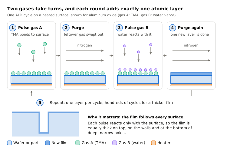
 13.4Atomic layer deposition (ALD)Coats a surface one atomic layer per cycle with alternating gasesOpen the lesson
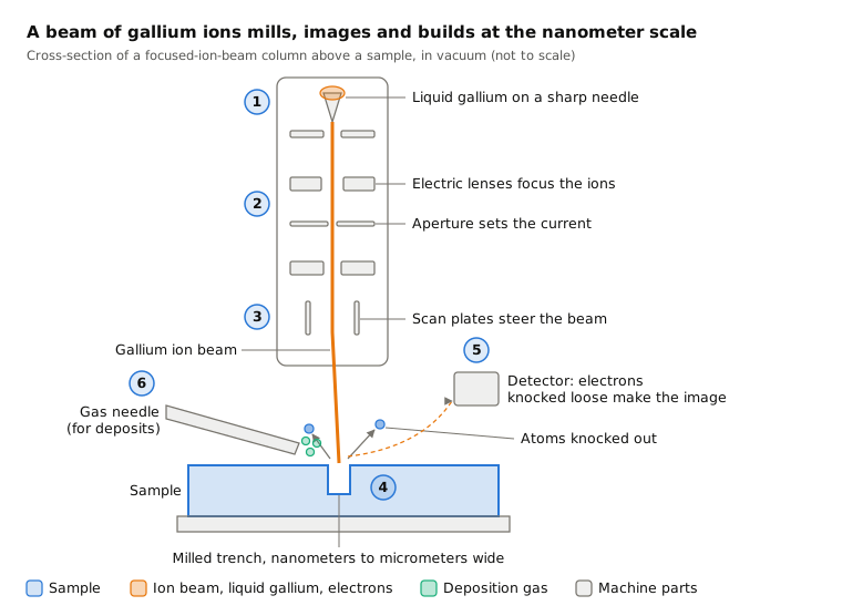
 13.5Focused ion beam (FIB)Mills or adds material with a beam of ions under a microscopeOpen the lesson
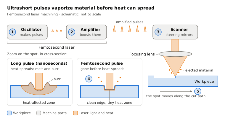
 13.6Femtosecond laser machiningRemoves material with ultrashort laser pulses, without meltingOpen the lesson
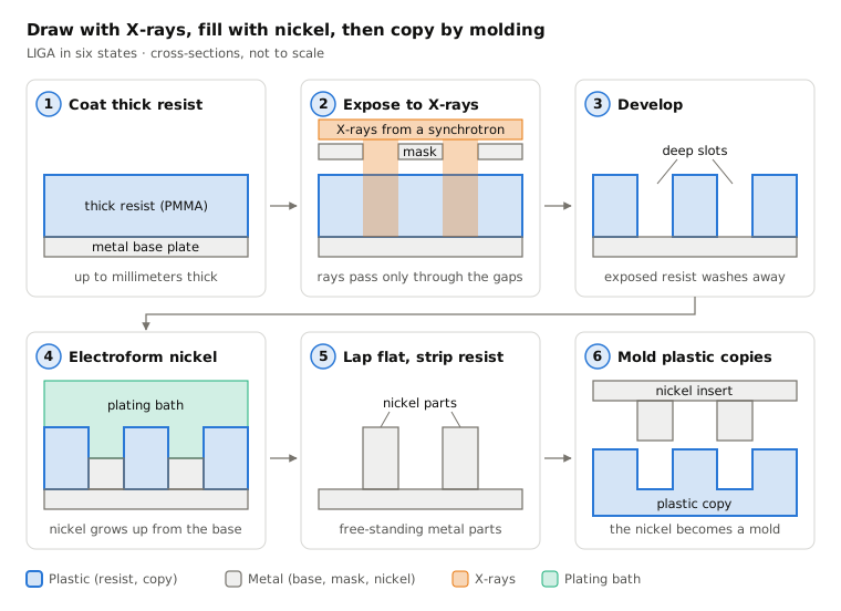
 13.7LIGADraws deep slots with X-rays or UV, fills them with nickel, then molds copiesOpen the lesson
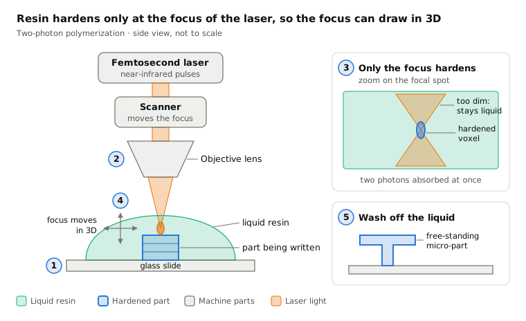
 13.8Two-photon polymerizationHardens resin only at a laser focus to print 3D micro-partsOpen the lesson
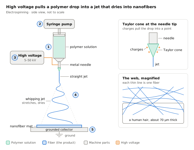
 13.9ElectrospinningPulls a polymer jet into nanofibers with high voltageOpen the lesson
Try it
Put AI to work in your CAD.
Model parts, generate drawings and automate the repetitive work inside your CAD software.