

Photolithography
Projects a pattern with light onto a light-sensitive coating, then etches it
Photolithography prints patterns onto a silicon wafer with light, much like developing a photo through a stencil. It draws the billions of transistors and wires on a computer chip, one layer at a time. Every chip in your phone went through it dozens of times.
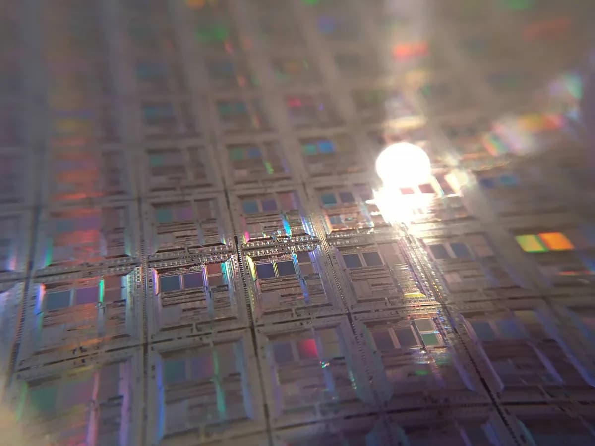
How it works
Spin-coat the resist. The wafer already carries a thin layer to be patterned, such as silicon oxide or metal. A few drops of photoresist (a light-sensitive liquid plastic) land on it, and the wafer spins at thousands of rpm, leaving an even film about a micrometer thick or less. A short bake dries it.
Align and expose. A mask (a glass plate carrying one layer's pattern in chrome, also called a reticle) is lined up with the patterns already on the wafer, to within a few nanometers on advanced chips. UV light shines through its clear parts, and a lens shrinks the image, typically four times, onto the resist. The machine, called a stepper or scanner, repeats this field by field across the wafer.
Develop. A developer liquid washes over the wafer. With the most common positive resist, the areas hit by light dissolve, leaving openings shaped like the mask's clear areas.
Etch. In a plasma etcher (a chamber of electrically charged gas), the plasma eats away the layer only where the resist is open; elsewhere the resist shields it. Instead of etching, the openings can also receive new material or implanted atoms.
Strip. The leftover resist is removed with solvents or an oxygen plasma. The pattern now exists in the layer itself.
Repeat. A new layer is added and the cycle starts again with the next mask, each pattern aligned to the ones below. An advanced chip goes through dozens of these cycles.
Key facts
- Materials
- Silicon wafers coated with photoresist; also glass, compound semiconductors and circuit boards
- Typical parts
- Flat patterns stacked layer by layer: transistors, wiring, sensors, display backplanes
- Part size
- Wafers up to 300 mm across; one exposure covers a field of about 26 × 33 mm
- Precision
- About a micrometer with simple lab aligners; tens of nanometers with 193 nm laser light; near 10 nm with EUV (13.5 nm) light
- Surface finish
- Leaves no texture of its own; patterned wafers shimmer in rainbow colors
- Batch size it suits
- Mass production: one mask set serves thousands of wafers, each holding hundreds to thousands of chips
- Tooling and machine cost
- Lab mask aligners: tens to hundreds of thousands of dollars; EUV scanners: hundreds of millions; an advanced mask set: millions
- Speed
- A production scanner exposes roughly 100–300 wafers per hour, one layer each
Strengths and limits
Strengths
- Patterns a whole wafer in parallel: billions of features at once
- Reaches nanometer-scale detail with modern scanners
- Very repeatable: the backbone of all chip production
- Very low cost per transistor at high volume
Limits
- Extremely expensive machines, masks and cleanrooms
- The wavelength of the light limits the finest detail
- Only flat layers; 3D structures come from stacking dozens of them
- Needs dust-free, vibration-free rooms under yellow light
Where it's used
- ElectronicsProcessors, memory chips, camera image sensors
- DisplaysThe transistor grid behind LCD and OLED screens
- Sensors and MEMSAccelerometers, microphones, pressure sensors
- PhotonicsLED chips, laser diodes, light guides on chips
- Circuit boardsCopper tracks, patterned with dry-film resist
- ResearchMicrofluidic "lab-on-a-chip" devices
How to recognize it
- The patterns are invisible to the eye. The finest lines are thousands of times thinner than a hair and need an electron microscope to see. They hide inside every chip in your phone, laptop and car, and behind every pixel of your screen.
- Rainbow shimmer. Tilt a bare wafer or chip die under light and it flashes rainbow colors: its regular patterns split light the way a CD does.
- Yellow-lit rooms. In factory photos, the lithography area glows yellow, because the resist ignores yellow light.
- Circuit boards. The fine copper tracks on a green circuit board were also defined by light through a mask, at a much coarser scale.
Compare with
Watch it
TED-Ed · A short animated overview of chipmaking and where lithography fits
Branch Education · Detailed 3D animation of every fab step, including the scanner
Conformable Decoders · Real lab photolithography, step by step
ASML · How the most advanced scanners make their EUV light
See real photos
- Wikipedia: Photolithography — diagrams of the steps and photos of lithography equipment
- Wikimedia Commons photo search
Remember
- Photolithography prints a whole chip layer at once, like developing a photo through a stencil.
- Coat, expose, develop, etch, strip, then repeat: dozens of cycles per chip.
- Shorter-wavelength light prints finer details, which is why EUV machines exist.
More in Micro- and nanofabrication
All 100 processes
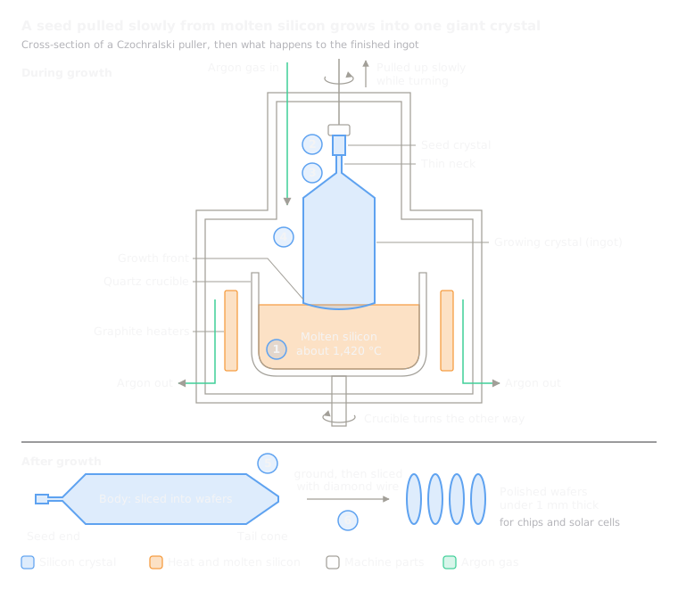 13.1Czochralski crystal growth (silicon wafers)Pulls a giant single crystal of silicon slowly out of a meltOpen the lesson
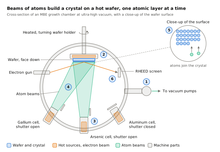
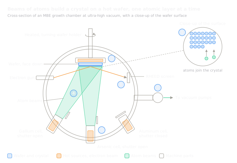 13.3Molecular beam epitaxy (MBE)Grows a crystal one atomic layer at a time from beams in ultra-high vacuumOpen the lesson
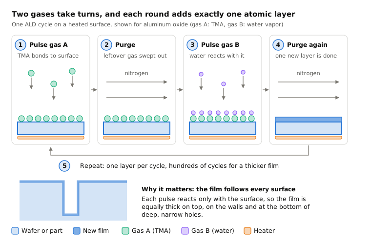
 13.4Atomic layer deposition (ALD)Coats a surface one atomic layer per cycle with alternating gasesOpen the lesson
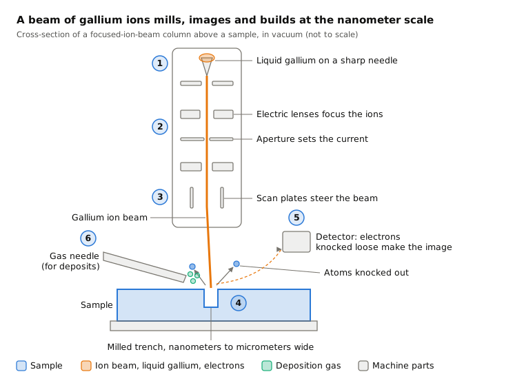
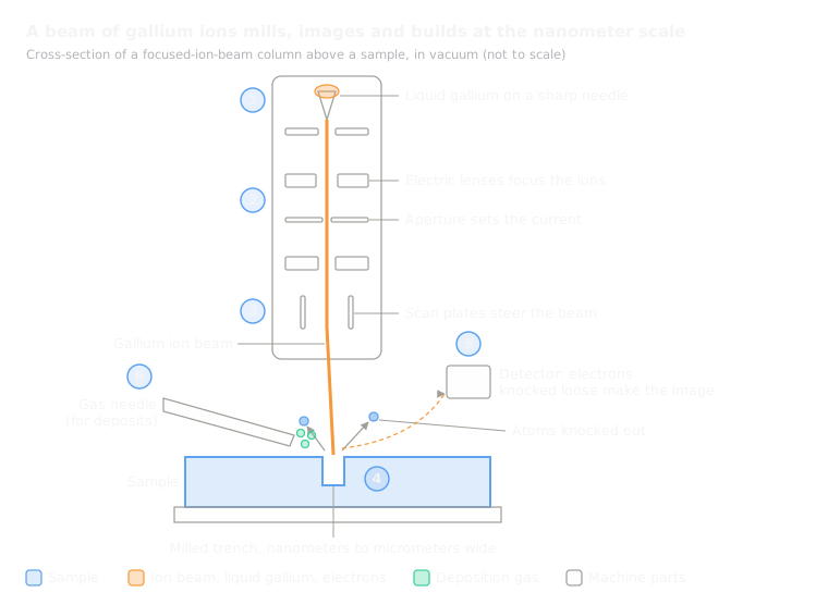 13.5Focused ion beam (FIB)Mills or adds material with a beam of ions under a microscopeOpen the lesson
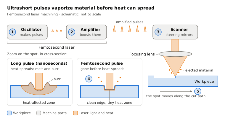
 13.6Femtosecond laser machiningRemoves material with ultrashort laser pulses, without meltingOpen the lesson
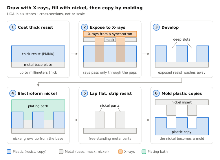
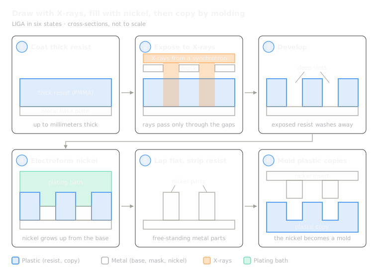 13.7LIGADraws deep slots with X-rays or UV, fills them with nickel, then molds copiesOpen the lesson
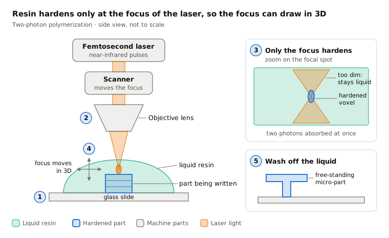
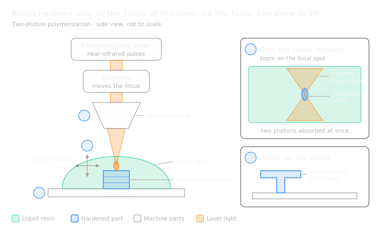 13.8Two-photon polymerizationHardens resin only at a laser focus to print 3D micro-partsOpen the lesson
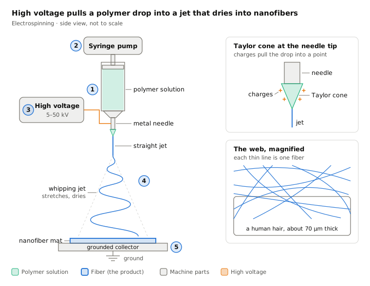
 13.9ElectrospinningPulls a polymer jet into nanofibers with high voltageOpen the lesson
Try it
Put AI to work in your CAD.
Model parts, generate drawings and automate the repetitive work inside your CAD software.